
Energy Band Theory : The Best way to explain Semiconductors.
Introduction to Energy Band Theory.
Have you ever wondered why copper carries electric current easily, while rubber does not? Or why silicon, which is neither a good conductor like copper nor a strong insulator like rubber, is used to make computers and smartphones? The answer lies deep inside the material, in the way its electrons are allowed to have and exchange energy. This is where energy band theory becomes important.
In a single isolated atom, electrons can occupy only certain specific energy levels. You can imagine these levels like steps on a staircase. An electron can stand on one step or another, but it cannot normally stand between the allowed steps. However, a solid contains an enormous number of atoms packed close together. When these atoms interact, their individual energy levels split into a huge number of very closely spaced levels. These closely packed levels form what we call energy bands.
Energy band theory is a model used in solid state physics to explain how electrons behave inside solids and why different materials have different electrical properties. It helps us understand the difference between conductors, semiconductors, and insulators by looking at the allowed and forbidden energy states available to electrons. The two most important energy bands are the valence band and the conduction band. The valence band contains electrons that are generally involved in the bonding and structure of the material. The conduction band contains higher-energy states where electrons can move more freely through the solid and contribute to electrical conduction.
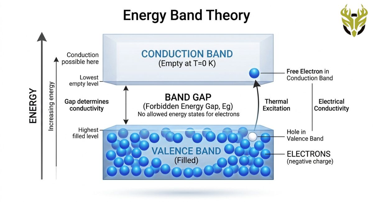
Between these bands, there may be an energy range in which electrons cannot normally exist. This region is called the forbidden energy gap, or simply the band gap. The size of this gap is extremely important because an electron must gain enough energy to cross the gap and reach an available conducting state. You can think of the band gap like a hill between two valleys. Electrons in the lower valley represent the valence band. The higher valley represents the conduction band. If the hill is very small, electrons can cross it relatively easily. If the hill is very large, crossing becomes much more difficult.
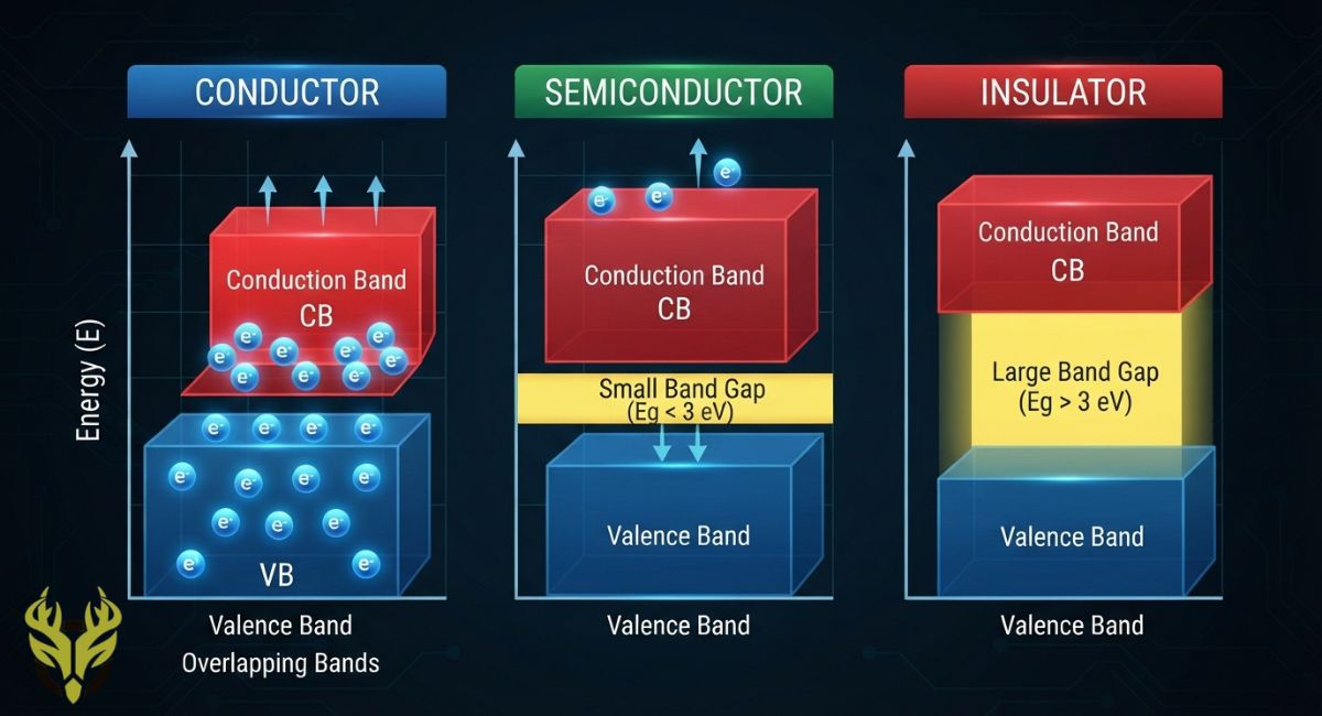
This simple picture helps explain the three major types of materials. In a conductor, electrons have readily available states for conduction, so electric current can flow easily. In an insulator, a large energy gap makes it difficult for electrons to reach conducting states. In a semiconductor, the gap is relatively small, so electrons can be promoted into conducting states under suitable conditions such as increased temperature, light, or electrical energy.
What Is Energy Band Theory?
Energy band theory explains the behavior of electrons in a solid by describing the ranges of energy that electrons are allowed or forbidden to have.
In a single atom, electrons occupy discrete energy levels. But when many atoms come close together, their electron states interact. The original energy levels split into many closely spaced levels, forming bands.
Between some bands there are energy ranges where electrons cannot normally exist. These regions are called forbidden energy gaps or band gaps.
How Do Energy Bands Form?
Think about two identical atoms placed far apart. Each atom has its own set of electron energy levels. As the atoms move closer together, their electrons begin to interact. Now imagine bringing not two atoms together, but a huge number of atoms—perhaps billions or more—to form a solid. Each atomic energy level splits into a very large number of slightly different energy levels.
Because these levels are extremely close together, they appear almost like a continuous energy band.
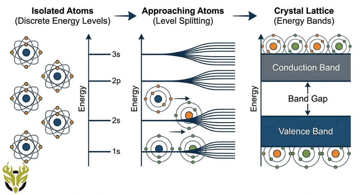
A simple way to imagine this is a row of houses. One house has only a few rooms, but imagine thousands of similar houses built next to each other. The individual rooms are still separate, but together they form a huge organized structure. Similarly, individual atomic energy levels combine into bands when many atoms form a solid.
Valence Band.
The valence band is the highest energy band that is normally occupied by electrons at very low temperatures.
The electrons in this band are generally associated with the outer electrons of atoms and with bonding within the solid. The behavior of the valence band is especially important because electrons may gain energy and move into higher-energy states, allowing electrical conduction to occur.
Conduction Band.
The conduction band is an allowed energy band in which electrons can move through the solid more freely and contribute to electrical conduction.
When electrons receive enough energy to move into available conduction-band states, they can respond to an electric field and produce an electric current. This is why the relationship between the valence band and conduction band is so important.
Forbidden Energy Gap.
Between the valence band and conduction band there may be an energy range in which electrons cannot normally exist. This is called the forbidden energy gap, or simply the band gap.
The size of this gap strongly influences the electrical behavior of a material.
The larger the relevant energy barrier for creating mobile charge carriers, the more difficult it generally is for electrons to contribute to conduction. In a semiconductor, the band gap is small enough that thermal energy, light, or other energy sources can promote some electrons into conducting states.
Energy Band Theory of Conductors.
In a conductor, electrons can move relatively easily because there are available energy states near the electrons that can participate in conduction.
In many metals, the valence and conduction bands overlap, or a partially filled band is present. Therefore, electrons do not need to overcome a large forbidden gap before they can respond to an electric field. This is why metals such as copper, silver, and aluminum conduct electricity well.
Simple Idea.
Conductor → electrons can move easily → high electrical conductivity
Energy Band Theory of Insulators.
In an insulator, the valence band is normally filled while the conduction band is separated from it by a large band gap.
An electron would need a large amount of energy to move from the valence band into the conduction band. Under ordinary conditions, very few electrons can make this transition, so electrical conduction is extremely weak.
Materials such as glass, rubber, and many ceramics are good examples of electrical insulators.
Simple Idea.
Insulator → large band gap → electrons have difficulty reaching conducting states
Conductor vs. Semiconductor vs. Insulator
| Property | Conductor | Semiconductor | Insulator |
| Band gap | Zero, overlapping, or effectively absent for conduction | Small | Large |
| Electron movement | Easy | Controlled | Difficult |
| Electrical conductivity | High | Moderate/controllable | Very low |
| Temperature effect | Conductivity generally decreases with temperature | Conductivity generally increases with temperature | Usually remains very low |
| Examples | Copper, silver, aluminum | Silicon, germanium | Glass, rubber, ceramics |
What Happens When an Electron Gains Energy?
Suppose an electron is in the valence band. If it receives enough energy, it can cross the band gap and enter the conduction band.
The electron then becomes a mobile charge carrier.
At the same time, the electron leaves behind an empty state in the valence band. This vacancy is called a hole.
So, in a semiconductor, electrical conduction can involve both:
Electrons in the conduction band
and
Holes in the valence band
A hole behaves like a positive charge carrier because neighboring electrons can move into the empty state, effectively causing the hole to move in the opposite direction.
Role of Band Gap.
The band gap is one of the most important features of a semiconductor.
If the band gap is small, electrons can be promoted to the conduction band more easily. If the band gap is large, much more energy is required. For example, when a semiconductor absorbs light with sufficient photon energy, an electron can be excited across the band gap. This principle is important in solar cells, photodetectors, LEDs, and other electronic and optical devices.
Energy Bands and Temperature
Temperature also affects the behavior of electrons in solids.
When a material becomes warmer, its particles gain thermal energy. In a semiconductor, this additional energy can allow more electrons to cross the band gap and enter the conduction band. As a result, the number of mobile charge carriers increases.
This is why the electrical conductivity of many semiconductors increases as temperature rises, which is opposite to the usual trend in metals.
Energy Bands and Doping
One of the most useful features of semiconductor physics is that we can deliberately change the electrical properties of a semiconductor by adding carefully selected impurities.
This process is called doping.
When certain impurities are added, the semiconductor becomes n-type or p-type.
- In an n-type semiconductor, electrons are the majority charge carriers.
- In a p-type semiconductor, holes are the majority charge carriers.
Doping does not simply add random particles to the material. It changes the available electronic states and makes it easier for charge carriers to participate in electrical conduction.
Intrinsic Semiconductor.
An intrinsic semiconductor is a pure semiconductor without intentionally added impurities.
Pure silicon is a common example. Each silicon atom has four valence electrons and forms covalent bonds with neighboring silicon atoms. At very low temperatures, most electrons remain involved in these bonds, so there are very few free charge carriers.
When the temperature increases, some electrons gain enough thermal energy to break away from their covalent bonds. These electrons become free electrons and can move through the crystal.
When an electron leaves its bond, it creates an empty space called a hole. The hole behaves like a positive charge carrier.
Therefore, in an intrinsic semiconductor:
n=p
where:
n = concentration of free electrons
p = concentration of holes
In simple words:
Intrinsic semiconductor = pure semiconductor → electrons and holes are produced naturally in equal numbers.
Example
Pure silicon (Si) and pure germanium (Ge) can behave as intrinsic semiconductors.
Extrinsic Semiconductor.
An extrinsic semiconductor is a semiconductor whose electrical properties have been deliberately changed by adding a very small amount of impurity.
This process is called doping.
Think of pure silicon as a quiet road with relatively few cars. If we add carefully selected atoms, we can greatly increase the number of available charge carriers. This gives us much better control over the electrical conductivity of the material.
Extrinsic semiconductors are divided into two main types:
- n-type semiconductor.
- p-type semiconductor.
-
n-Type Semiconductor
An n-type semiconductor is produced by adding a pentavalent impurity, meaning an impurity atom with five valence electrons, to a pure semiconductor such as silicon.
Common donor impurities include phosphorus, arsenic, and antimony.
Silicon normally uses its four valence electrons to form four covalent bonds. When a phosphorus atom replaces a silicon atom, four of its five valence electrons participate in bonding. The fifth electron is only weakly attached and can become a free electron.
Therefore, doping creates many additional free electrons.
Main Charge Carrier
In an n-type semiconductor:
Majority carriers = electrons Minority carriers = holes
The impurity is called a donor impurity because it provides an extra electron.
Easy Memory Trick
n-type → negative → electrons
So:
n-type semiconductor = extra electrons
-
p-Type Semiconductor.
A p-type semiconductor is produced by adding a trivalent impurity, meaning an impurity atom with three valence electrons, to a pure semiconductor.
Common acceptor impurities include boron, aluminum, and gallium.
When a boron atom replaces a silicon atom, it has only three valence electrons available for bonding. One bond is therefore missing an electron, creating a hole.
The hole can move through the crystal as neighboring electrons move to fill the empty position.
Main Charge Carrier
In a p-type semiconductor:
Majority carriers = holes Minority carriers = electrons
The impurity is called an acceptor impurity because it can accept an electron.
Easy Memory Trick
p-type → positive → holes
So:
p-type semiconductor = extra holes
Intrinsic vs. Extrinsic Semiconductors.
| Feature | Intrinsic Semiconductor | Extrinsic Semiconductor |
| Purity | Pure semiconductor | Doped with impurities |
| Doping | No intentional doping | Intentional doping |
| Charge carriers | Electrons and holes | Electrons or holes dominate |
| Conductivity | Relatively low | Higher and controllable |
| Types | No separate types | n-type and p-type |
| Majority carriers | Electrons = holes | Electrons or holes |
| Example | Pure Si, pure Ge | Phosphorus-doped Si, boron-doped Si |
What Is Electrical Conduction?
Electrical conduction is the movement of electric charge through a material when an electric field is applied.
In a semiconductor, the charge can be carried by:
Electrons and holes
An electron carries a negative charge:
q=−e
where
e=1.602×10^−19 C
A hole behaves as a positive charge carrier:
q=+e
So, semiconductor current can be thought of as having two contributions:
I=Ie+Ih
where Ie is the electron current and Ih is the hole current.
Conduction by Electrons.
In a semiconductor, some electrons can gain enough energy to move from the valence band into the conduction band.
Once an electron is in the conduction band, it can move relatively freely through the crystal.
Imagine a crowded hallway. If one person is able to leave the crowded room and enter the hallway, that person can move from one side to the other. Similarly, a conduction-band electron can move through the semiconductor and contribute to electric current.
When an external electric field is applied, the electrons acquire a small average drift velocity opposite to the direction of the electric field because electrons have negative charge.
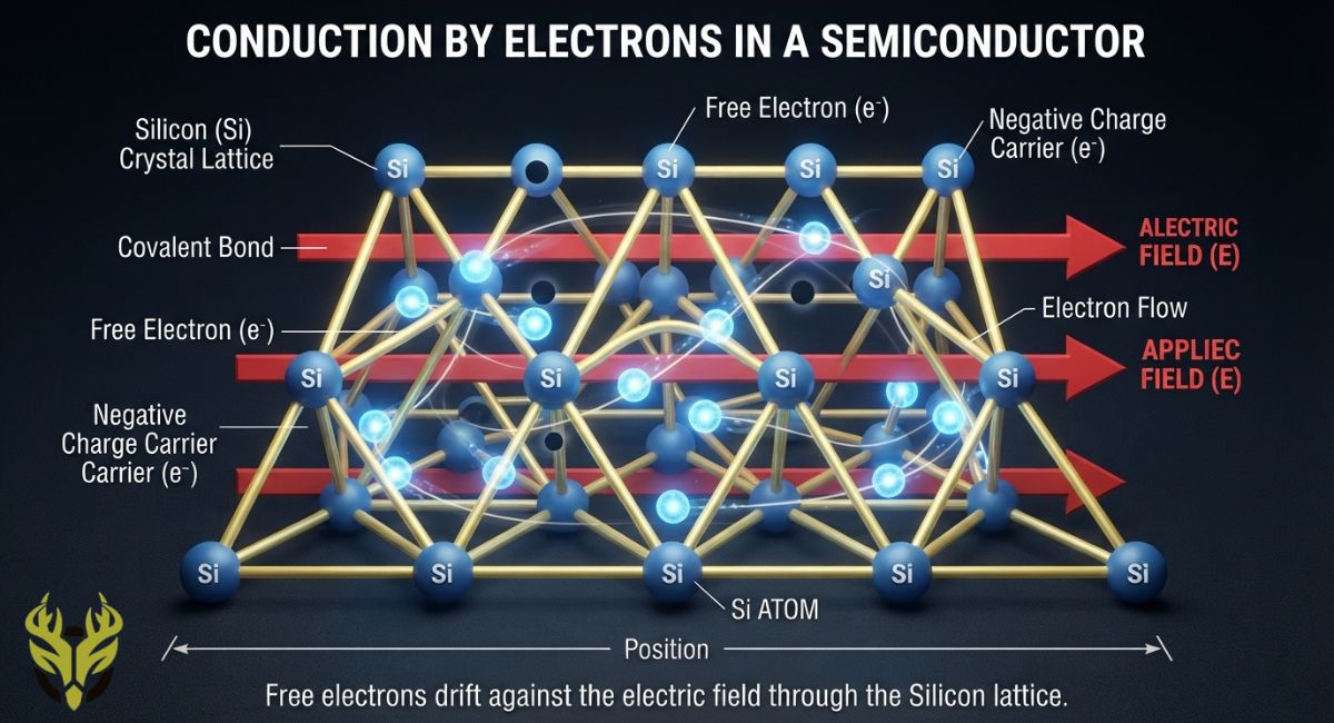
The electron drift current density can be expressed as:
Jn=neμnE
where:
Jn = electron current density
n = electron concentration
e = magnitude of electron charge
μn = electron mobility
E = electric field
Conduction by Holes.
A hole is an empty state left behind when an electron leaves the valence band.
At first, it may seem strange to say that an empty space can carry electric current. But imagine a row of seats with one empty seat. If people keep moving into the empty seat, the empty position appears to move in the opposite direction.
The same idea applies to holes.
When a neighboring valence electron moves into a hole, it leaves another hole behind. Repeated movement of electrons makes the hole appear to move through the crystal.
Because a hole behaves as a positive charge carrier, its drift direction is opposite to that of electrons.
The hole current density is:
Jp=peμpE
where:
Jp = hole current density
p = hole concentration
e = magnitude of electron charge
μp = hole mobility
E = electric field
Why Do Holes Move?
A hole does not represent a separate physical particle like an electron. Instead, it represents an empty allowed electron state in the valence band.
Suppose we have three neighboring atoms:
Electron → Electron → Hole
An electron next to the hole can move into it:
Electron → Hole → Electron
The hole has effectively moved in the opposite direction.
If this process continues:
Hole → → →
the hole appears to travel through the semiconductor and contributes to electrical conduction.
This is why physicists treat holes as positive charge carriers even though the actual microscopic particles moving in the valence band are electrons.
Electron and Hole Conduction Together.
In a semiconductor, both electrons and holes can contribute to the total current.
The total current density is:
J=Jn+Jp
Therefore:
J=neμnE+peμpE
or:
J=e(nμn+pμp)E
This equation shows that semiconductor conductivity depends on both the number of charge carriers and their mobility.
The electrical conductivity is:
σ=e(nμn+pμp)
Therefore:
J=σE
This is the semiconductor form of the familiar relationship between current density, conductivity, and electric field.
Electron and Hole Conduction in n-Type Semiconductors
In an n-type semiconductor, donor impurities provide additional electrons.
Therefore:
n≫p
Electrons are the majority carriers, while holes are the minority carriers.
The electron contribution to current is therefore much larger than the hole contribution under ordinary conditions.
Simple Picture
n-type → many electrons → electron conduction dominates
Electron and Hole Conduction in p-Type Semiconductors
In a p-type semiconductor, acceptor impurities create conditions that produce many holes.
Therefore:
p≫ n
Holes are the majority carriers, while electrons are the minority carriers.
The hole contribution to current is therefore usually much larger.
Simple Picture
p-type → many holes → hole conduction dominate.
n-Type vs. p-Type Conduction.
| Property | n-Type Semiconductor | p-Type Semiconductor |
| Majority carrier | Electrons | Holes |
| Minority carrier | Holes | Electrons |
| Main impurity | Donor | Acceptor |
| Typical dopant | Phosphorus | Boron |
| Dominant conduction | Electron conduction | Hole conduction |
| Charge of majority carrier | Negative | Positive |
What Happens When an Electric Field Is Applied?
Suppose an electric field is applied across a semiconductor.
The electrons experience a force opposite to the direction of the electric field because they have negative charge. The holes behave as positive charge carriers and drift in the same direction as the electric field.
So we can remember:
Electrons drift opposite to E Holes drift in the direction of E
Interestingly, both movements produce conventional electric current in the same direction.
This is because conventional current is defined as the direction in which positive charge would move.
Why Are Electrons Usually More Mobile Than Holes?
Electrons in the conduction band generally have greater mobility than holes in the valence band.
This happens because the effective mass and interaction of electrons and holes with the crystal lattice are different.
Typically:
μn>μp
for many common semiconductor materials. For silicon, for example, electrons generally move more easily through the crystal than holes.
This means that even if electron and hole concentrations were comparable, their contributions to conductivity would not necessarily be equal.
Electrical Conduction in an Intrinsic Semiconductor
In an intrinsic semiconductor, electrons and holes are generated in pairs.
Therefore:
n=p=ni
where ni is the intrinsic carrier concentration.
The conductivity becomes:
σ=eni(μn+μp)
Both electrons and holes therefore contribute to conduction.
As temperature increases, more electron-hole pairs are generated, so the number of charge carriers increases and the conductivity of the semiconductor generally increases.
Electrical Conduction in an Extrinsic Semiconductor
In an extrinsic semiconductor, impurities are deliberately added to control the number of charge carriers.
For an n-type semiconductor:
n≫ p
so electron conduction dominates.
For a p-type semiconductor:
p≫ n
so hole conduction dominates.
This controlled electrical behavior is the foundation of modern semiconductor technology.
Easy Way to Remember
The entire concept can be remembered with four simple ideas:
Electron → negative charge → moves opposite to electric field
Hole → positive charge → moves with electric field
n-type → electrons are majority carriers
p-type → holes are majority carriers
The most important equation is:
σ=e(nμn+pμp)
It tells us that the conductivity of a semiconductor depends on how many electrons and holes are available and how easily they can move.
Conclusion.
Energy band theory answers a question that seems simple on the surface but reaches deep into how modern technology actually works: why does copper conduct electricity effortlessly, while rubber blocks it completely, and silicon sits precisely in between? The answer isn’t about the material itself so much as the space between its valence and conduction bands, a gap so small in a conductor it barely exists, so large in an insulator that electrons rarely cross it, and just right in a semiconductor to be controlled on demand.
That controllability is exactly why silicon runs your phone instead of copper or rubber. Through doping, engineers can deliberately tip a semiconductor toward extra electrons or extra holes, building the n-type and p-type materials behind every diode, transistor, and solar cell in existence. Understanding energy bands isn’t just theoretical physics. It’s the quiet foundation underneath nearly every piece of modern electronics you touch every single day.
Frequently Asked Questions
Q. What is energy band theory?
Energy band theory is a model in solid state physics explaining how electrons behave inside solids, using allowed energy bands and forbidden gaps to distinguish conductors, semiconductors, and insulators.
Q. What is the difference between the valence band and conduction band?
The valence band holds electrons involved in atomic bonding, while the conduction band holds higher-energy electrons free to move and carry electric current. The gap between them determines a material’s conductivity.
Q. What makes silicon a semiconductor instead of a conductor or insulator?
Silicon has a small band gap, small enough that heat, light, or electrical energy can push electrons from the valence band into the conduction band, unlike a conductor’s overlapping bands or an insulator’s large gap.
Q. What is a hole in semiconductor physics?
A hole is an empty space left behind when an electron leaves the valence band. It behaves like a positive charge carrier, since neighboring electrons shifting to fill it makes the gap itself appear to move.
Q. What is doping in semiconductors?
Doping is deliberately adding impurity atoms to a semiconductor to control its conductivity, creating either an n-type semiconductor (extra electrons) or a p-type semiconductor (extra holes).
Q. What is the difference between intrinsic and extrinsic semiconductors?
An intrinsic semiconductor is pure, with electrons and holes produced in equal numbers naturally. An extrinsic semiconductor has been doped with impurities, making either electrons or holes the dominant charge carrier.
Q. Why does a semiconductor’s conductivity increase with temperature, unlike a metal’s?
Higher temperature gives more electrons enough energy to cross the band gap into the conduction band, increasing charge carriers. Metals behave oppositely, since rising temperature disrupts electron flow instead of adding carriers.